Optoelectronics has become one of the most important markets in the semiconductor industry. Once seen as a specialized domain for niche applications, optoelectronic technologies are now enabling massive shifts in the way data is created, transmitted, and consumed across cloud computing, artificial intelligence (AI), automotive, telecommunications, consumer electronics, and other applications. Many emerging devices and systems currently shaping our world rely on optoelectronics to run faster, consume less power, and connect reliably.
At the same time, AI is not only creating unprecedented demand for optoelectronic devices—connecting data centers and high-bandwidth networks—but it’s also influencing their design and manufacture. AI’s exponential growth has made optoelectronics both a critical enabler and a technology sector under tremendous pressure to continue advancing. How will manufacturers keep up with the complexity, cost, and performance requirements that AI’s evolution demands?
One of the answers is wet-processing techniques. Advanced cleaning and etching steps are foundational to producing high-performance optoelectronic devices. Precision, repeatability, and efficiency at the wafer level can make the difference between a viable technology and one that fails to scale. With its decades of wet-processing systems expertise, JST is uniquely positioned to serve this market. Our solutions are designed not only to handle the materials and geometries of optoelectronic devices but also to anticipate the sustainability, throughput, and cost-of-ownership requirements of an AI-driven world.
How AI Is Driving Optoelectronics
Optical interconnects replacing copper in data centers
AI is not only a consumer of optoelectronics—it’s also a catalyst. AI workloads involve massive data throughput, low-latency requirements, and intense computational demands. To keep pace, optical interconnects are rapidly replacing traditional copper interconnects in data centers. At the same time, silicon photonics and compound semiconductor technologies are being adopted to deliver higher speeds and lower energy consumption.
Manufacturing challenges and scaling requirements
Every AI model trained today requires exponentially more data and more compute power than the one before it. This wave of demand transforms the requirements on the manufacturing floor. Processes that were once sufficient at a smaller scale must now achieve new levels of uniformity and reproducibility. Throughput must improve without sacrificing quality. And every efficiency gain, whether in water use, chemical consumption, or footprint, contributes directly to customer competitiveness.
A Key Market for JST
Compound semiconductor challenges
Optoelectronics is more than just another vertical market—it is a natural fit for our core strengths in wet processing. Optoelectronic devices often involve challenging materials such as indium phosphide (InP), gallium nitride (GaN), and silicon carbide (SiC). These compound semiconductors have very different properties from traditional silicon, and they require equally distinct approaches to cleaning and etching. Our process expertise, combined with our flexible equipment platforms, enables customers to achieve results that are difficult or impossible to match with conventional methods.
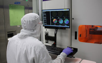
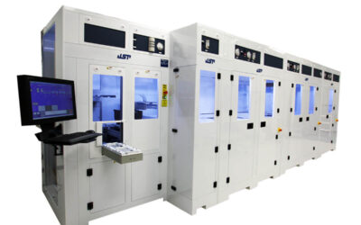
Single-wafer wet processing system for AI and optoelectronics
Our Ospray single-wafer wet process system is a prime example of this alignment. Optoelectronics is a market often caught in the gap between laboratory-scale research and high-volume manufacturing. Many equipment suppliers have focused their attention either on very large, multi-chamber platforms designed for mainstream silicon fabs or on small tools suited only for research. This has left optoelectronic device makers underserved. Ospray fills this gap by offering a platform that delivers high performance, excellent uniformity, and repeatability while remaining accessible for both R&D and scaled production.
Customers consistently report that Ospray delivers superior process results in optoelectronics applications—better uniformity, more repeatable outcomes, and lower chemical consumption. The system’s footprint is also smaller than competitive alternatives, a critical factor in cleanroom environments where space translates directly to cost. In side-by-side comparisons, our tools have proven not only technically capable but also operationally efficient, providing a tangible advantage in yield and cost of ownership.
Building for Efficiency and Sustainability
Reducing water and chemical use in wet processing
Another defining feature of JST’s technology is its attention to efficiency and sustainability. Semiconductor manufacturing has always been resource-intensive, and optoelectronics is no exception. As fabs worldwide face increasing scrutiny over water and chemical use—especially in regions like Europe where regulators are tracking consumption—equipment suppliers must design tools with efficiency in mind.
Cost of ownership improvements
We have taken significant steps in this area. Recent upgrades to its dryers have reduced tank volumes by as much as 15 percent, directly cutting both water and chemical usage. Modular system designs make it easier for customers to scale capacity without unnecessary waste, while throughput improvements ensure that processes run faster and with less energy. Taken together, these innovations can improve the cost of ownership by at least 15 percent compared to prior generations, a meaningful advantage in a market where margins are constantly under pressure.
For customers, the benefits are both economic and environmental. Lower water and chemical use translates to reduced operating expenses, but it also supports corporate sustainability goals and compliance with regional regulations. In this way, we help our partners achieve performance, cost, and environmental targets simultaneously.
Differentiation Through Flexibility
Tailored customer solutions
Rather than imposing a one-size-fits-all approach, we work closely with our customers to tailor solutions. These modifications may be as simple as adding a customized bracket or as complex as adapting software interfaces to better display process data. Whatever the scale, the willingness to adjust to customer needs is a hallmark of our business model.
Wafer size versatility
This flexibility is particularly important in optoelectronics, where device structures and materials vary widely. While some fabs are pushing silicon carbide to 200 mm, many compound semiconductor applications remain at 150 mm or smaller. Our tools are capable of handling wafer sizes from 3-inch research substrates to 300 mm production wafers, offering unmatched versatility. This ensures that you can continue to use our platforms as your needs evolve, avoiding the disruption of switching tools midstream.
On the Horizon
AI-driven demand in data centers, telecom, and automotive
The future of optoelectronics is inseparable from the future of AI. As computing becomes more data-intensive and connectivity becomes more ubiquitous, optoelectronic devices will be asked to do more than ever before. Data centers will depend on optical interconnects to keep pace with AI workloads. Telecommunications will rely on advanced photonics to deliver faster, more reliable networks. And automotive systems will increasingly adopt sensors and lidar that depend on precise optical performance.
Next-generation wet processing platforms
Meeting these demands requires innovation not only at the device level but also at the manufacturing level. Wet processing will remain central to that effort, and we will play a vital role in enabling the next generation of optoelectronic technologies. By advancing flagship platforms such as the Ospray single-wafer system and our next-generation Front Linear Automated (FLA) wet bench, we are preparing our customers for the challenges ahead.
For companies navigating the complexities of AI-driven markets, we offer not just tools but a true partnership—helping customers turn their ideas into a high-yield, sustainable reality.
Contact JST today to learn how we can help you bring your next project to fruition.