Scaling Optoelectronic Device Fabrication with HBr and InP
As optoelectronic devices continue to scale in performance and complexity, we are seeing a fundamental shift in how critical fabrication steps, such as etching, must be approached. Whether enabling high-speed data transmission through photonics or supporting next-generation sensing and communication systems, compound semiconductors such as indium phosphide (InP) demand precision that traditional processes can struggle to achieve.
Manufacturers are also under pressure to improve yields, reduce variability, and lower the cost of ownership. While batch processing has been historically used, JST has developed a proprietary HBr process that enables high uniformity within-wafer and wafer-to-wafer.
This is where the combination of hydrogen bromide (HBr) chemistry and InP material systems becomes particularly powerful. By pairing HBr wet etching with InP substrates, JST is enabling a new level of uniformity, repeatability, and manufacturability for optoelectronic devices.
Indium Phosphide: Material Advantages and Fabrication Challenges
InP is uniquely suited for optoelectronic applications due to its intrinsic combination of direct bandgap, high electron mobility, low noise, and strong thermal stability. These characteristics make InP ideal for use in lasers, photodiodes, and high-frequency devices operating across a wide temperature range.
At the same time, InP-based devices face fabrication challenges, as they are highly sensitive to surface damage, profile distortion, and process variability. Even small inconsistencies in etch depth or uniformity can translate into performance degradation or yield loss. The etch process must therefore remove material with the highest possible precision and selectivity, while minimizing impact on the underlying structure.
Why Hydrogen Bromide: Selectivity, Plasma-Free Removal, and Lower Cost of Ownership
HBr offers a compelling combination of attributes that align well with the needs of InP processing. Taken together, these characteristics make the two highly complementary:
- Excellent chemical selectivity when etching InP. This allows us to remove targeted material layers while preserving adjacent structures – an essential requirement for complex device architectures.
- Support for high etch uniformity. Uniformity is one of the most critical parameters in semiconductor manufacturing, particularly for optoelectronics. We have demonstrated that HBr-based wet etching can achieve within-wafer uniformity in the 1–2% range—significantly better than the ~5% typically seen in comparable systems.
- Low-damage material removal. Unlike plasma-based etching, which relies on ion bombardment, wet etching with HBr is purely chemical. This eliminates plasma-induced defects and preserves the integrity of sensitive InP surfaces.
- Faster and more cost-effective processing. Compared to many dry-etch approaches, HBr facilitates processing at lower cost and higher speeds, making it attractive for high-volume manufacturing environments.
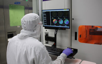
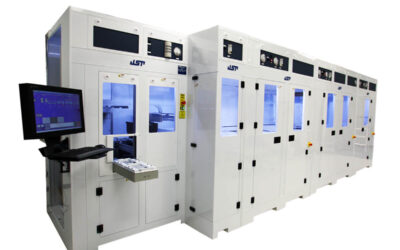
Precision Single-Wafer Wet Processing on the JST Ospray Platform
Despite these advantages, wet etching produces an isotropic etch profile, which can lead to undercutting and feature distortion if not carefully controlled. In addition, achieving consistent chemical distribution across the wafer surface is non-trivial. Variations in flow rate, nozzle design, and wafer rotation can all introduce non-uniformities that impact device performance.
Historically, batch processing methods have struggled to meet these requirements at scale. As wafer sizes increase and device tolerances tighten, even small process variations can become unacceptable. This is the core problem we set out to solve.
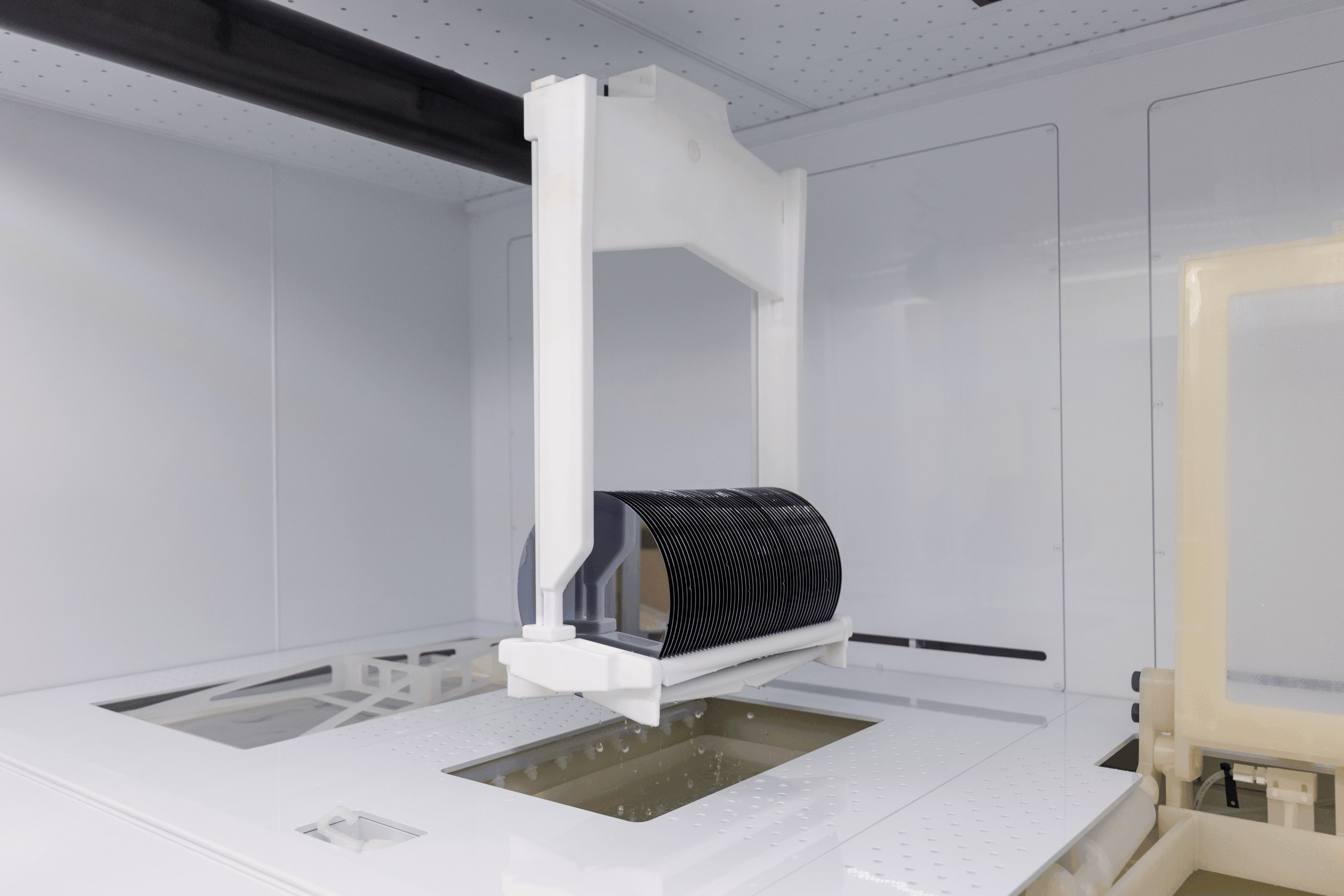
To fully unlock the benefits of HBr for InP etching, we developed a precision single-wafer wet-processing approach that provides tight control over every aspect of the process. At the center of this approach is our Ospray single-wafer processing platform, which is specifically engineered to deliver uniform chemical application and repeatable process conditions.
Rather than relying on batch immersion, we use a controlled spray-based delivery system in which HBr is applied through a precisely engineered nozzle. This allows us to:
- Ensure even chemical distribution across the wafer
- Control flow rates (typically in the 100–250 ml/min range)
- Optimize nozzle patterns and angles
- Synchronize wafer rotation for uniform exposure
This level of control is critical for managing the inherently isotropic nature of wet etching. By tightly regulating how and where the chemistry interacts with the wafer, we can maintain feature integrity while achieving the desired etch profile.
Achieving 1–2% Etch Rate Uniformity: Repeatability, Yield, and Scalability
The results of this approach speak for themselves. Through extensive process development and design-of-experiments (DOE) work, we have consistently achieved etch rate uniformity in the 1–2% range, with some measurements as low as 1.24%. These results represent a significant improvement over conventional systems, where uniformity often hovers around 5%.
More importantly, this performance is not a one-off result. Our repeatability data shows that we can maintain this level of uniformity across multiple wafers and process conditions, enabling:
- Consistent pattern fidelity
- Reduced device variability
- Higher overall yields
From a manufacturing perspective, the combination of HBr chemistry, InP substrates, and precision single-wafer processing delivers several key benefits, including higher yield, lower cost of ownership, improved device performance, and inherent scalability, enabling support of larger wafer sizes and tighter process tolerances as the industry evolves.
What’s Next for InP Photonics Manufacturing
As optoelectronics continues to expand into new applications—from high-speed data communications to advanced sensing—the demands on fabrication processes will only increase.
We believe that the combination of HBr wet etching and InP substrates represents a foundational capability for meeting these demands. But chemistry alone is not enough. The real differentiator lies in how that chemistry is delivered, controlled, and integrated into a production environment.
By combining deep process expertise with precision single-wafer technology, we are enabling manufacturers to achieve the uniformity, repeatability, and efficiency required for next-generation devices. It’s not just about making HBr and InP work together – it’s about making them work reliably, at scale, and with the performance the industry demands.
Contact JST today at info@jstmfg.com to learn how we are advancing precision single-wafer processing for the next frontier of semiconductor manufacturing.