For decades, silicon has defined the semiconductor industry, but as electrification accelerates across sectors, silicon’s performance limits are becoming more visible. Silicon carbide (SiC) and gallium nitride (GaN) have emerged as critical alternatives, offering higher voltage tolerance, better thermal performance, and faster switching characteristics. These advantages make them particularly valuable in applications such as electric vehicles, renewable energy systems, utility grids, and increasingly power-hungry data centers.
For decades, silicon has been the foundation of the semiconductor industry. Today, however, the global transition toward electric mobility, advanced energy generation, and higher-efficiency power systems is exposing the practical limits of silicon-based devices. Wide-bandgap materials such as silicon carbide (SiC) and gallium nitride (GaN) are emerging as transformative technologies, enabling higher operating voltages, superior thermal performance, and significantly faster switching speeds. As a result, SiC and GaN are becoming central to next-generation power electronics across electric vehicles, renewable energy infrastructure, utility-scale power systems, and high-performance data centers.
Leading Market Drivers
While performance is the primary driver, the markets adopting SiC and GaN differ sharply from those pushing the boundaries of advanced CMOS logic. They do not require extreme dimensional scaling, but they do demand reliable substrates, stable process flows, and consistent, cost-effective manufacturing. This shift brings new challenges to the fab floor—challenges that play directly into JST’s long-standing strengths in wet processing and surface preparation.
The rise of SiC and GaN also highlights manufacturing constraints, particularly around substrate cost and availability. SiC and GaN are expensive, especially as the industry moves from 3-inch to 4-inch wafers in pursuit of better economies of scale. Maintaining substrate purity and crystal quality is difficult, and cleaner, more uniform surfaces are necessary to support high-performance epitaxy and device reliability. Although SiC’s opaque material characteristics introduce differences in handling compared with silicon, the core requirements around cleaning and preparation remain well aligned with JST’s established process capabilities.
How JST Is Enabling the Shift
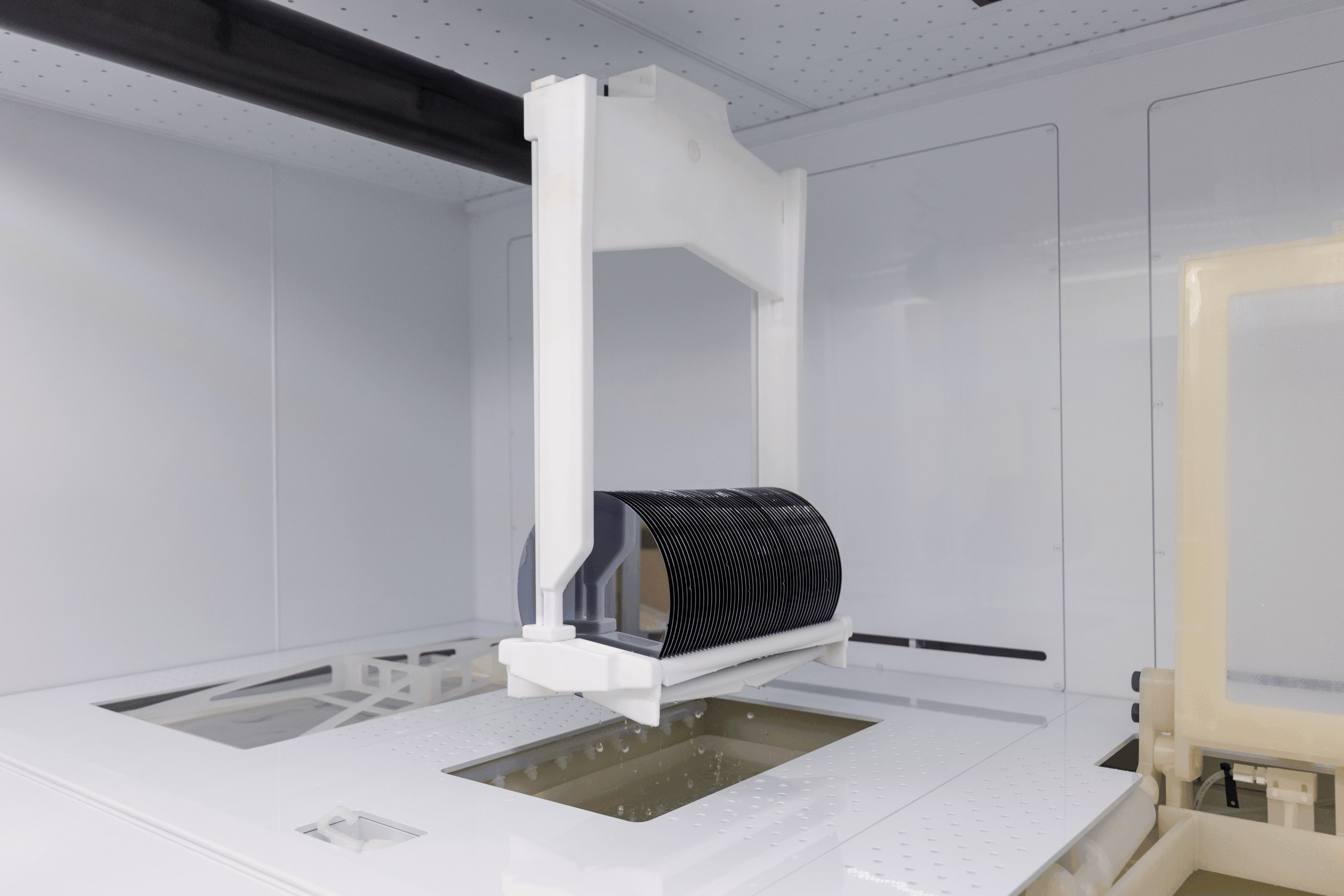
JST’s equipment platforms are inherently adaptable for wide-bandgap materials—making them particularly valuable for manufacturers who need cost-effective high performance. Most SiC and GaN workflows benefit from batch immersion systems, and JST’s Front Linear Automated (FLA) wet bench platform is well suited to these demands. Features such as megasonics for effective particle removal, Marangoni drying for defect-minimizing surface finishing, and advanced chemical concentration control help ensure consistent results and optimize cost of ownership.
In addition, JST’s systems are designed with smaller footprints, optimized exhaust requirements, and overall efficiency improvements that benefit price-sensitive wide-bandgap markets. Vertical integration further strengthens JST’s position. By manufacturing many of its own components, JST can offer improved quality control, shorter lead times, and lower lifecycle costs—key advantages for customers working to accelerate SiC and GaN production without overextending budgets.
Beyond equipment, JST supports customers through its application lab, where process development, best-known-method refinement, and hands-on collaboration take place. This capability helps device makers and foundries validate new approaches, adjust surface-prep strategies, and adopt new materials more confidently. Although the wide-bandgap market is still maturing, JST has already demonstrated success with related materials such as indium phosphide on its Ospray single-wafer platform, reinforcing its credibility and deep knowledge base.
Future Outlook
Looking ahead, SiC and GaN will continue to gain traction as global demand for electrification grows. The expansion of EV charging corridors, improvements in battery technology, and the ongoing push for more efficient power infrastructure will set the pace for the next decade. As these markets scale, the manufacturers who succeed will prioritize stable processes, reliable equipment, and lower cost of ownership.
JST is well positioned to support this transition. With decades of experience in wet processing, a proven portfolio of adaptable platforms, and a commitment to efficiency and quality, JST offers the tools and expertise needed to help customers accelerate their SiC and GaN manufacturing strategies.
Contact JST today at info@jstmfg.com to learn how our wet-processing systems and application expertise can support your SiC and GaN production roadmaps.