Browse Products
Wet Process Semiconductor Applications
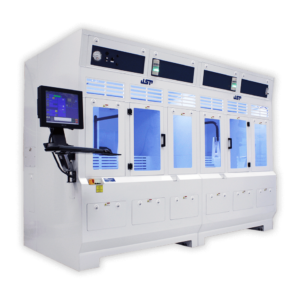
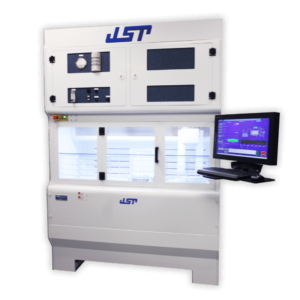
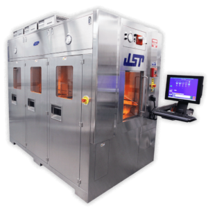
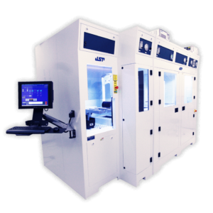
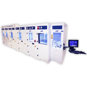
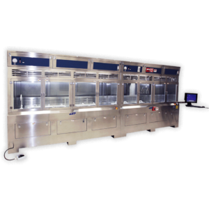
With more than 40 years of experience, JST has extensive knowledge of wet process semiconductor applications. We aligned the development of our process modules to fulfill the needs of common wet processes performed within each wet bench we manufacture.
Our expertise as semiconductor equipment manufacturers includes onsite plastics, contract metal fabrication, and mechanical and electrical assembly. Only quality, reliable, cleanroom-approved components are utilized in our designs to provide long-term reliability and minimal maintenance. We collaborate with customers to provide custom lab, fab, and HVM requirements solutions.
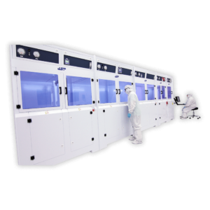
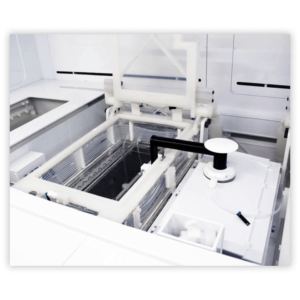
JST’s Class 10 applications lab enables our customers to develop wet process applications using real-world tools, modules, and chemicals. This, coupled with our partnerships with various chemical vendors, results in reduced chemical usage, optimized cleanroom footprints, and efficient automation for improved throughput—providing maximum return on investment.